Indigenous memory technology adoption for 180 nm CMOS production: A national milestone in semiconductor R&D
The natural world is analog while computing is digital. Computers perceive the natural world through sensorchips whose output is analog. The analog output is converted into the language of computers through a digitizer chip or an analog to digital converter (ADC). Foundries mass-produce these chips. Ideally, these chips should be identical but manufacturing variations produce tiny offsets which are revealed upon testing. This renders a large fraction of chips useless. The tiny offset may be stored in memory once and applied to the output afterward to make each imperfect chip, “perfect”! Using this method,generic chips can now be designed and application-specific offsets added to make expensive custom chip design redundant, saving time and money for the user.
Chip technology gaps became the focus of investigation for Indian researchers asthe demand for semiconductors increased inthe country and globally. The Government of India took cognizance of the significance of R&D in innovation-drivensemiconductor manufacturing.TheyimprovedR&D capacity by buildingCentres for Excellence in Nanoelectronics (CENs);the firstones being atIIT Bombay and the Indian Institute of Science. This led to a transformed semiconductor research ecosystem making the country a major contributor to electron device-related research.
The next challenge was to translate research to manufacturing. The semiconductor manufacturing ecosystem in India is led by Semi-Conductor Laboratory (SCL), Mohali, Department of Space, Government of India, and is the most advanced semiconductor manufacturing fab (a large facility with cleanroom environments used to produce memory chips) in the country.
“The success of the “Digital India” initiative by the Government of India has underpinnings in our country’s ability to manufacture electronics hardware. The focus on electronics hardware including integrated circuits or chips is key to strengthen R&D primarily in the Space and Defense sectors. Development of standards, product design or IP development, and semiconductor manufacturing are increasingly important. Improving India’s participation in this area is a major priority for R&D in India. The partnership between IIT Bombay and SCL to establish this memory technology for the first time demonstrates the augmented potential for semiconductor research in the country”, said Prof. K. VijayRaghavan, Principal Scientific Adviser (PSA) to the Government of India.
IIT Bombay partnered with SCL to successfully demonstrate CMOS 180nm based production-ready 8-bit memory technology. IIT Bombay invented the one-time programmable (OTP) memory based on ultra-thin deposited silicon dioxide (a few atoms thick) instead of the existing gate oxide-based OTP technology. In contrast to the high voltage required by gate oxide breakdown (a popular OTP memory), IIT Bombay’s memory chip requires less power and chip-area as the need for boosted voltage supply is avoided.“Memory technology is critical to data security. It is essential for present and future Indian Fabs. To infuse innovation, translating memory technology from research to manufacturing is the key to compete globally and serve locally to establish a vibrant semiconductor ecosystem. The OTP Memory Technology Adoption for Trimming Application by the joint IIT Bombay – SCL Chandigarh teams is a pioneering step in this direction. It will be a gamechanger by enabling secure memory and encryption hardware for the country.” Dr. V.K. Saraswat, Member, NITI Aayog.
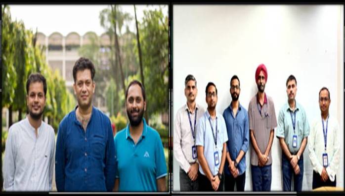
The team at IIT Bombay was supported by the Department of Science and Technology’s Intensification of Research in High Priority Area (IRHPA).Aspects of the work were funded byMeitY/DST’s Nanoelectronics Network for Research and Applications (NNetRA)supportsthe memory application,DST-Advanced Manufacturing Technologies, and the Office of PSA for hardware security.The team at IIT Bombay partnered with IITDelhi,SETS Chennai, and DRDOfor hardware encryption.
“One out of 100 ideas make the journey from Lab to Fab. The exacting process of exceeding 95% yield requires an unrelenting multi-disciplinary team supported by a world-class R&D infrastructure to form an enduring collaboration. Once successful such technology opens possibilities of touching countless lives, in this case, through chips with a tiny memory,” said Prof. Udayan Ganguly, who leads the team at IIT Bombay.